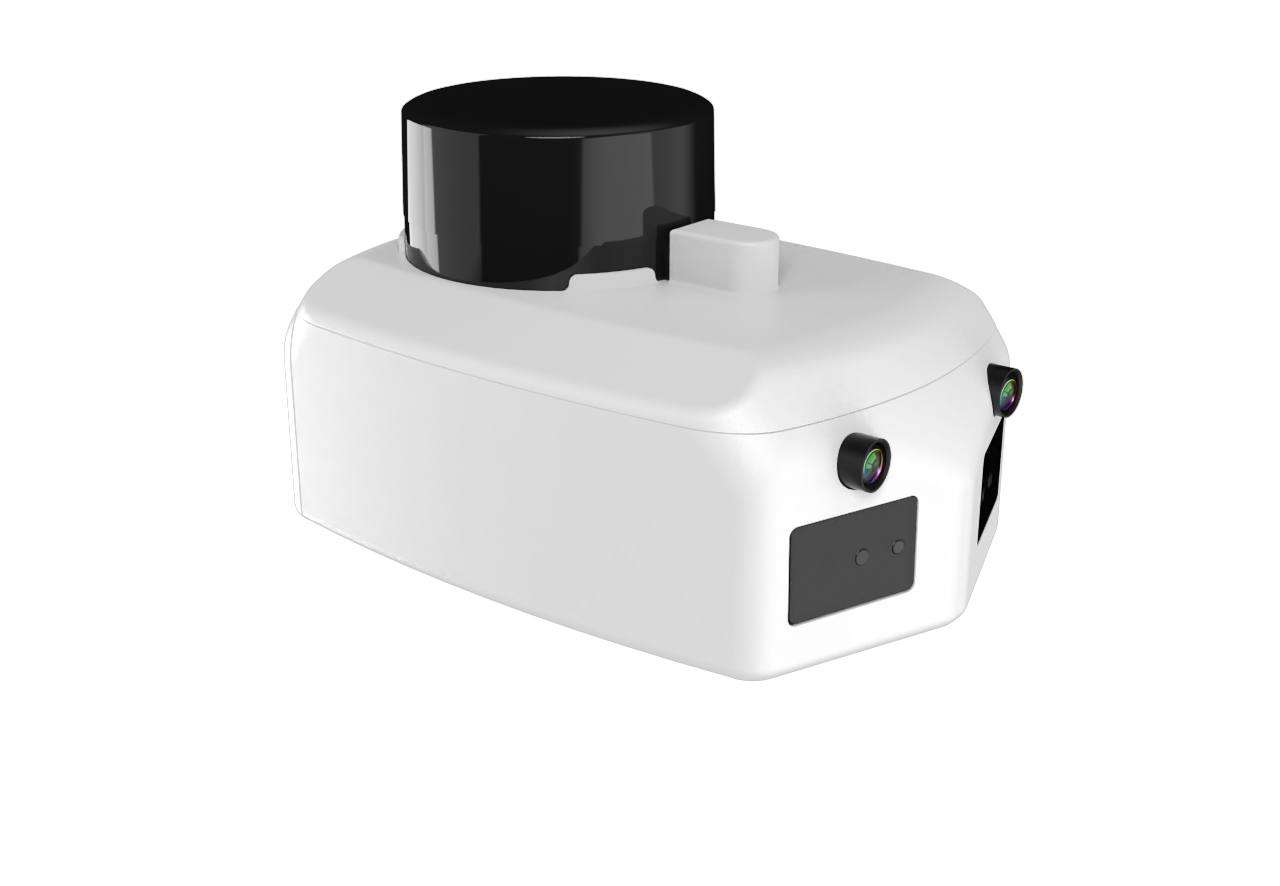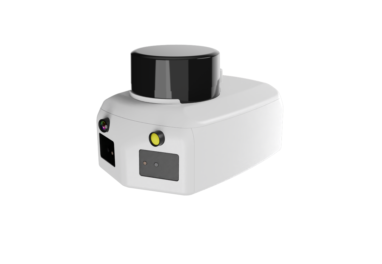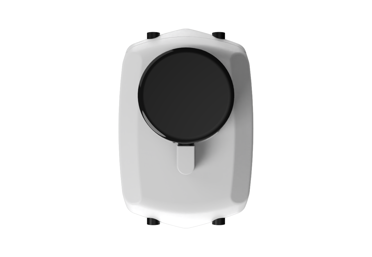
IOT Enclosure
Branding, DesignIoT enclosure design is a packaging problem with five competing masters: the PCB, the antenna, heat, water, and the tooling budget.
The challenge. Design a compact plastic enclosure for an IoT device that protects the electronics, maintains wireless performance, manages heat, and assembles fast — while staying within a startup-friendly tooling cost.
Design and engineering. The enclosure was architected around the PCB from day one. Boss and snap-fit locations were coordinated with the board layout so the PCB drops in and locks without fasteners. The housing keeps plastic-only zones around the antenna area — no metallic finishes or ribs creating detuning — to preserve RF performance. Passive thermal venting was integrated into the geometry where it’s invisible at normal viewing angles, and the two-part clamshell closes with a continuous tongue-and-groove seal path, upgradeable to a gasket for IP54+ variants.
DFM. Uniform walls, generous draft, snap-fits designed within material strain limits for repeated service opening, and a parting line placed along a styled feature line so it reads as intentional design rather than a molding artifact.
Result. Production CAD, 2D drawings, and DFM documentation — an enclosure engineered for real-world deployment, not just a render.
Building an IoT or electronics product? Enclosure design for PCBs is my core specialty — 200+ shipped products. [Start here.]